Semiconductor fabrication

From silicon surface to device structure.

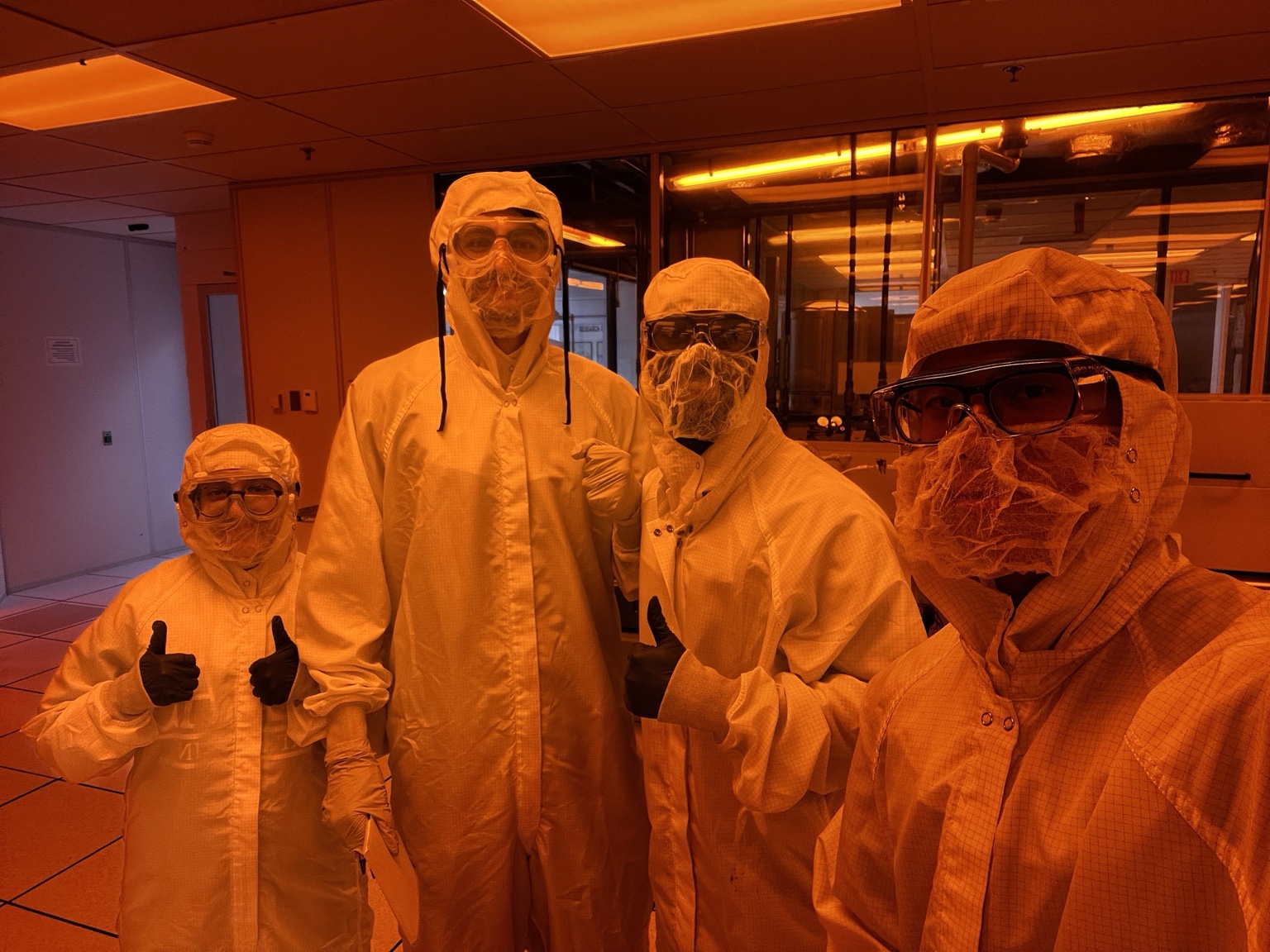
I’m processing silicon wafers in the cleanroom as part of my semiconductor fabrication coursework. Each step connects a fabrication choice to the electrical behavior of the devices we’ll build and measure.

01

Completed

Wafer cleaning

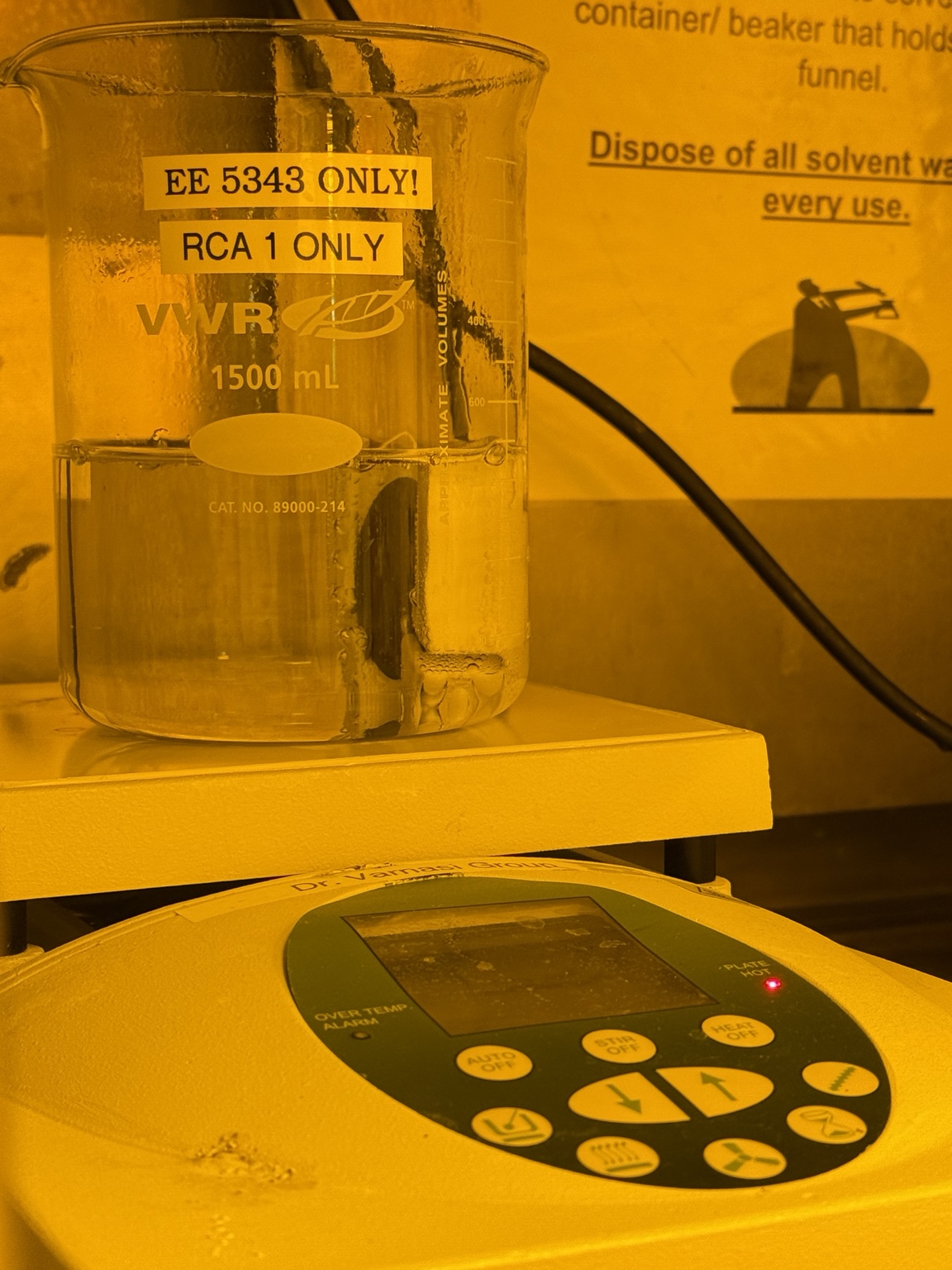
I cleaned 2-inch (100) p-type silicon wafers using RCA-1 and RCA-2 solutions, followed by deionized water rinsing and nitrogen drying. The sequence removes organic residue, some metal contamination, and mobile ions before oxide growth.
02

Completed

Spin-on doping & phosphorus diffusion

I measured the starting sheet resistance of silicon wafers with a four-point probe, cleaned and dried their surfaces, then spin-coated a phosphorus dopant. After baking the coating, I used a tube furnace for predeposition and repeated drive-in steps. I measured sheet resistance between steps to track how the thermal process changed the wafers’ electrical properties.

03

Up next

Dry thermal oxidation

Next I’ll grow silicon dioxide (SiO₂) on the cleaned wafers in an oxygen atmosphere using a 1000 °C tube furnace. I’ll then measure oxide thickness by ellipsometry and compare growth with the Deal–Grove model.

04

Later in the process

MOS capacitor fabrication

The oxidized wafers will be used to make MOS capacitors, linking the oxide layer and its measured thickness to a device structure.